Underlying Theory
The first task at hand was to understand the underlying theory of the project to motivate the goal and also to begin to understand how to tackle the design. The core of the project is to identify intermodulation distortion. This is not a new concept but using software defined radio for the task is a relatively recent development in the RF field. The simple reason to identify IMD products is that they are undesirable; to remove them you first need to identify them and they can also be used to quantify nonlinearity of a component. The project does not aim to counter these IMD products, but lay out a groundwork for identification with SDRs, a cheap and scaleable alternative to older custom analog circuitry. IMD is when 2 tones modulate in a nonlinear device and produce undesired new tones.

Fortunately, it is possible to predict the location of these IMD products as they are a function of the f1 and f2 (the two original tones). Many of the IMD products fall far enough away from the primary tones that they can be discarded with a bandpass filter but the third order distortion products fall too close to the original tones for this solution. These products can easily be misinterpreted as real data. One way to quantify the nonlinearity of a nonlinear device (for example an amplifier), is by its Third-Order Intercept point. This is a hypothetical point where the power of the third order IMD product reaches that of the fundamental components.
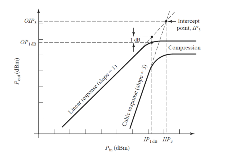
The reason the IP3 point is hypothetical is that the amplifier saturates before it can ever be met. It is still possible however to predict it and has proven to be a useful way to characterize nonlinearity. IP3 (or TOI) is valuable for low power amplifiers but for the high power amps to be used in this project, the metric will not be valuable. However, identification of IMD is still valuable.
Specifications / Requirements
The first task after defining a general system architecture and project goals was to create specifications. Given the open-ended nature of a proof-of-concept project, there was much flexibility in how to define requirements. Given the availability of components at no cost such as a Raspberry Pi 4b and Nexys-4 DDR FPGA, it was decided that it was acceptable to shape specifications around the hardware. With that in mind, the following is a list of specifications / system requirements:
- Only 1 Pair of Host and Co-processor
- 32k Point FFT
- With the storage available on the Nexys-4 DDR FPGA, it was determined that the largest possible FFT size that can be performed on two signals simultaneously is 32,768 points.
- 32k Point FFT
- Parallel Interface between Pi and FPGA
- In an effort to maximize throughput, a custom parallel interface is to be implemented.
- General Frequency Range Scalability
- The system must be functional for any range of signal frequencies
- Limitations are present due to the SDR but software will be scalable
- The system must be functional for any range of signal frequencies
Top Level Architecture
With the specifications and goal in mind, a top level architecture was developed.
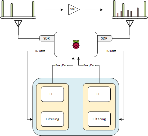
A single host will take the data from both SDRs and communicate with a coprocessor that performs the FFT and sends data back to the host.
Component Selection
As described above, a Raspberry Pi 4b was available for no cost as well as a Nexys-4 DDR FPGA. This leaves only the SDRs to be selected.
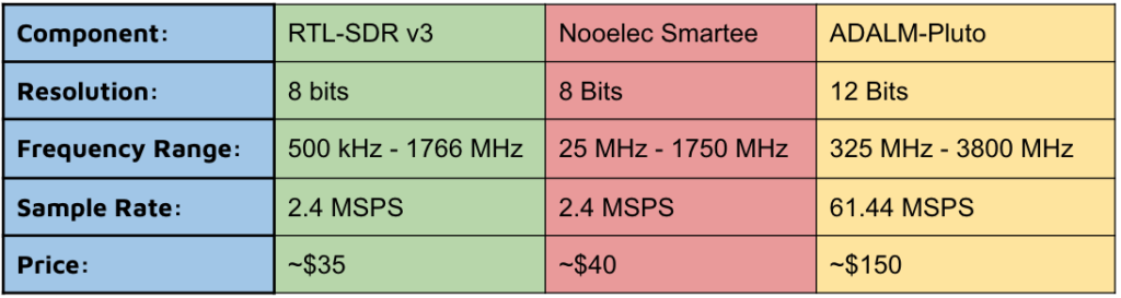
The above table details the specifications of some popular SDR models; the prices listed fluctuate partially on vendor and are based on bundle prices that involve some extra peripherals like cables and antennas. All the options listed have reasonable frequency ranges for the project needs so the primary concerns were frequency resolution, sample rate, and price. The importance of the resolution may be amplified in specific use cases but for the focus of this project, 8 bits per I or Q sample carries enough information. The sample rate is important as it defines the frequency bandwidth available for analysis at any sample time. The ADALM-Pluto greatly surpasses the RTL-SDR v3 and Nooelec Smartee in this regard, but if signals are chosen wisely for testing, 2.4 MHz of bandwidth is plenty. For these reasons, price became the primary consideration among these parts. The RTL-SDR v3 was chosen as it is the cheapest but an ancillary benefit is that it is used by many hobbyists and has a wide array of online resources.
Interface Design
As discussed in the project requirements, it was decided that a parallel interface was to be implemented between the Pi and FPGA.
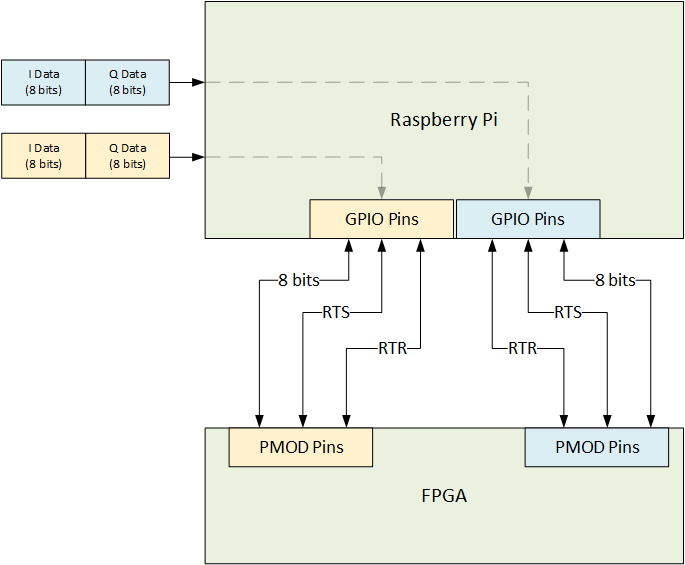
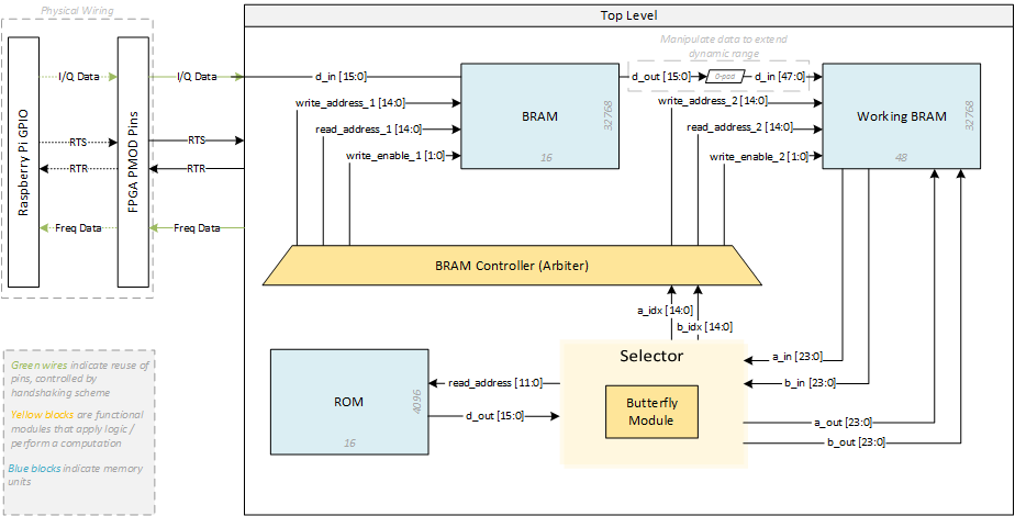
The above diagram shows how the design of the interface will be implemented. Since both SDRs will be processed at the same time, the number of GPIO pins and PMOD pins available on the Pi and FPGA respectively, limit the system to share 8 bits of data from each at a time. Each SDR will have 10 pins dedicated to it: 8 for data (I/Q information), and 2 for handshaking purposes. Each data pin will act as both input / output depending on which stage of the data transfer process is running.
The handshaking pins will take on the following structure:
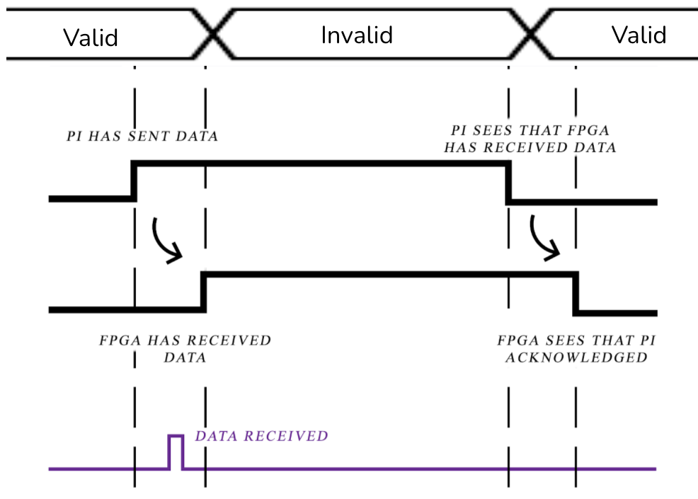
Due to the lack of clock synchronization between the Raspberry Pi and FPGA, a pair of standard ready to send and ready to receive signals cannot be used. In the case of the Pi transferring I/Q data to the FPGA, once the data from the buffer is conditioned and ready to send, the data GPIO pins will update. At the same time, the Pi will assert high to indicate it is ready to send. This will trigger the FPGA to read the data and once it is stored, will assert high to say it has received data. The Pi responds by going low again, to which the FPGA responds by also going low. This entire 4 stage cycle indicates that data has successfully been transferred from the Pi to the FPGA. The same structure will be used for data passing from the FPGA to the Pi, but the leading pin of the pattern swaps.
FFT Background
FPGA Design

The storage used by FPGA architecture defined is analyzed above for a Nexys-4 DDR FPGA. There should be 2 ROMs adding up to 2.6% (the figure will be updated).